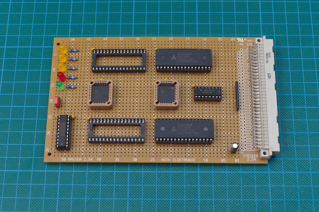
The Memory Board hosts the CFT’s main memory. Both volatile (RAM) and non-volatile (ROM, EPROM, EEPROM or Flash) memory may be accommodated on the board.
The original design of the board accommodates up to 1,024 kWords, but since this board is very simple, it is relatively easy to add another 512 or 1,024 kWords. Alternatively, two separate boards may be built to provide the full amount of memory for the computer.
The memory board is unsurprisingly designated MEM for consistency, although it is not a system device, and is unique.
C1.1. Design
The memory board follows the expanded, 21-bit CFT address space. It allows for up to 221 = 2,097,152 16-bit words. That's 2 MW for you.
The memory board provides:
- An address decoder that works in the extended memory address space.
- Two to four banks of memory.
- An optional buffer and status LEDs to indicate state. These are nearly useless when the computer operates at full speed, but they've been pretty handy for early debugging!
The current design implements two banks, independently configurable via jumpers. One bank is reserved for ROM, the other for RAM. The ROM bank accepts JEDEC-style ICs in 32-pin PLCC packages. It features a jumper to allow the Flash WE signal to be driven by the CFT in normal writes. This allows the ROMs to be reprogrammed in-circuit by either the DEBDebugging Front Panel (DFP) board or the CFT computer itself (provided, of course, the software to do so is running purely in RAM).
RAM banks are simpler, but they are built for 32-pin DIP packages. The RAM is static. It's not that building a DRAM state machine with address registration, row/column multiplexing, and refresh circuitry with bus synchronisation that doesn't cause the processor to block every 50 µs or so is harder than interfacing to static RAM. It's just that it's harder. And that size of static RAM is cheap enough not to be worth the extra 20 or so chips and debugging time.
In the current design, all banks are 16 bits by 4 Mbits, which makes 512 kWords. This design decision is partially responsible for the increased importance of the MBU card. The reason is simple: 4 Mbit devices were the cheapest option when I sourced them. Cheaper than smaller static or dynamic RAM, in fact! Initially, I was going to just let the upper 448 kW go to waste, but then I changed my mind. If I had 512 KW memory back in the Eighties, I could have killed any hardware designer who made it unusable. And would probably have to stand in line.
Since these chips are 8 bits wide, two chips are used in parallel to provide 16-bit word storage, forming two-chip memory banks.
C1.2. Theory of Operation
Access to the card’s facilities is possible via a standard address decoder built from an equally standard 74HC138 decoder. The 138 decodes AEXT6–7 (the 21st and 20th bits of the 21-bit extended address space) when MEM is asserted. These are decoded into one of four active-low chip select lines, RAMEN0, ROMEN0, RAMEN1 and ROMEN1 as follows:
| MEM | AEXT6–7 | Base address | RAMEN0 | RAMEN1 | ROMEN0 | ROMEN1 | Notes |
|---|---|---|---|---|---|---|---|
| 1 | XX | 1 | 1 | 1 | 1 | No memory transaction. | |
| 0 | 00 | 00:0000 | 0 | 1 | 1 | 1 | Bank 0: RAM Bank 0 selected. |
| 0 | 01 | 40:0000 | 1 | 0 | 1 | 1 | Bank 1: RAM Bank 1 selected. |
| 0 | 10 | 80:0000 | 1 | 1 | 0 | 1 | Bank 2: ROM Bank 0 selected. |
| 0 | 11 | C0:0000 | 1 | 1 | 1 | 0 | Bank 3: ROM Bank 1 selected. |
Expanded Address Format
For convenience, expanded addresses are listed not as weird 21-bit hex numbers, but as a colon-separated vector of 8-bit high order addresses (expanded scheme memory blocks) and 13-bit offsets in those memory blocks where a physical addressxx:yyyy is calculated by (xx << 13) | (yyyy & 0x1fff). We won't be bothering much with offsets in this discussion, though. The four chip select lines can optionally be routed via jumper sets to change each bank's base address. This is a remnant of when each MEM board would have had just one bank of 512 kW memory.
Each memory bank comprises a pair of either static 8-bit RAM ICs, or (in the current design) Flash EEPROM. The OE signals are driven by the CFT's R signals. The WE signals are driven by the W strobe. ROM banks intended to take Flash devices can have their WEsignals physically disconnected from W as a means of write protection. When connected, Flash devices require a particular ‘magic’ sequence of writes to erase chip ‘sectors’, and a separate sequence to allow rewriting. Thus, Flash memory cannot easily be overwritten by mistake. But let's not risk that: I'm keeping those jumpers disabled for now.
Each of the 4 Mbit devices accepts a 19-bit address. The top two bits of the 21-bit vector have been used already to decode a single memory bank. The address in the memory bank is the vector <AEXT0–5, AB0–12>, where AEXT0–5 represents the high order bits.
For debugging and testing, an optional inverting buffer shows the chip selection state of the board, along with R and W, to drive LEDs. As designed, the card uses four of the eight buffers. For a full four-bank card, another two may be used, along with additional LEDs and current-limiting resistors.
Expanded CFT Memory Map using the MEM board. Shows all four banks and their current contents. The memory board implements three of the four banks. Of these, only one RAM bank and the ROM bank are populated with memory currently. The remaining RAM bank (Bank 2) is not populated. The fourth bank, Bank 3, which is not implemented by the memory board, is reserved for memory mapped I/O like a graphics card.
C1.3. Customising the Card
The buffer and state-displaying LEDs are completely optional and may be left out entirely.
Additional banks may be fitted and attached to the appropriate lines of the address decoder. The constructed card already has one extra bank.
If smaller memories are used in either bank, any number of sockets may be installed, for whatever type of memory is available. The memory should have an SRAM-like interface, of course. JEDEC-standard pin-outs give more options and are preferable.
The CFT ROM detects memory via heuristics, not via DIP switches or hardwired settings, so any mapping of RAM and ROM will work. For turnkey operation, the MBU assumes there are at least 32 kW of ROM at the start of Bank 2, starting at 80:0000. Or, to be precise, that the 8 kW block at 83:0000–83:1FFF maps to ROM that contains valid boot code.
One benefit of colocating multiple banks of memory on the same card is that only one decoder chip is needed. This reduces chip count by one to three units, and also saves considerable amounts of board estate.
Please note that the two-bank design was intentional: when I initially designed the card, I assumed I'd need memory-mapped devices and decoding is much simpler if all memory blocks have the same size. 512 kWords of RAM and ROM should be enough for the CFT. I'll be happy if I use 128 kW of either.
C1.4. Implementation
The implementation of the memory board diverges from the schematics slightly. Since I built in three physical banks, only one memory board can be installed in the system. The bank selection jumpers were pointless in this case, so I never wired them.
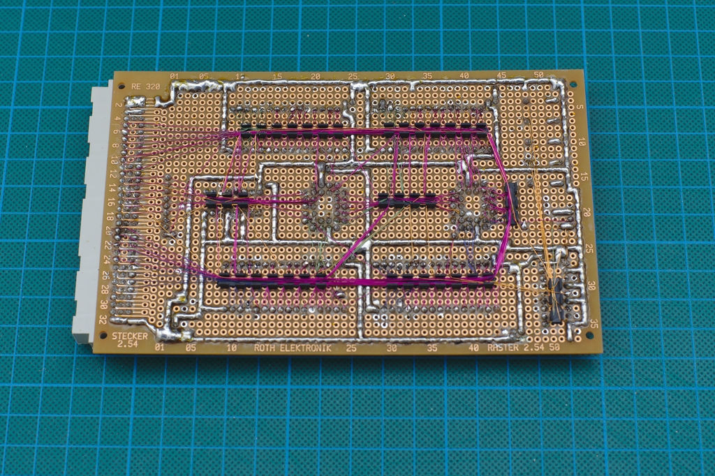
Physically, the memory board was implemented on a generic 160×100mm Perfboard using point-to-point soldering with enamel wire. This technique makes for very compact wiring, but is not as easy to debug issues or follow wire from pad to pad, and the result is not as æsthetically pleasing than it should be. In fact, it looks downright weird.
Bank 1 (the second RAM bank) is wired, but not yet populated. I need to order some SRAM chips.

The memory board as constructed. Note the sockets for the upper 512 KWords of RAM.

The underside of the memory board as constructed, with weird and ugly but convenient enamel wire prototyping.
C1.5. Schematics
The following page shows the full schematic drawing of the Memory Board (MEM) board, as implemented: three banks, an extra LED for the extra bank, and no jumpers. (other than a write-protect one for the Flash ‘ROM’).
Figure 6. Schematic of the MEM board, as actually wired.
