B4.1. Processor Implementation
The datapath is a lie, of course. Things are slightly more complex than that. The CFT processor includes a lot more units, and they work at a lower level than that. The processor is implemented on four 160×100mm 3U Eurocards, all attached to the computer bus and a processor-specific side-bus. The boards are named PB0 to PB3.
- Processor Board 0 (PB0):
- is the microcode sequencer board. Its most salient feature is the three ROMs containing the Microcode. It also holds the UPC, which points to the current microinstruction in a microprogram, decoders to select the read and write units on the IBus. These signals are all sent to the Front Panel, and signal buffers (some inverting) are included on board. There was some space left over, so PB0 is also where the Expansion Bus is terminated and conditioned. Miraculously, there was still space left over so recent revisions of the board include the UCB Extension.
- Processor Board 1 (PB1):
- contains the clock generator, reset logic, and most of the control unit, including the IR and Interrupt logic. The Data Bus Driver is here too.
- Processor Board 2 (PB2):
- this is a register board. It hosts the Major Registers. The Autoindex Logic is also here. The AB and Address Bus drive logic is here as well. Like the PB0, the board has a little spare space
- Processor Board 3 (PB3):
- the Arithmetic and Logic Unit (ALU) is implemented on this board. This is the logical place for the Overflow flag (V) and L registers, of course. In a last-minute decision to use up the board, the MBU extension (which was initially meant to be a separate board) was moved here too because I had trouble sourcing DIP versions of the 74HC670. Using SO16 chips, the extension fit neatly.
Why the weird numbering?
Initially, there were meant to be three processor boards (PB1–PB3) and a small Microcode daughterboard. There was no internal bus. Things didn't quite fit. I added an 80-pin internal bus which carries processor-specific signals, and moved the microcode store to its own board.B4.1.1. Technology
The whole point of the CFT is to make a computer by using discrete TTL chips. Early in the project I arrived at a decent clock speed of 4 MHz, but lots of operations have to happen within the 62.5 ns of a quarter clock period. So I switched to discrete CMOS chips, the HC family specifically. You get much better power consumption with CMOS, at the cost of somewhat less forgiving requirements: no floating inputs allowed for one.
Initial versions of the processor boards used through-hole chips. For reasons of speed (and to finally learn how to solder them), the processor board ended up being made out of SOIC chips. This increases the chip density quite a bit and allows us to have chips on both sides of the board. Passives are in 0805 packages for easy of soldering. There are also some small resistor packages and single gates in SOT23 packages. ROMs (technically, Flash devices) in PLCC32 packages are among the few through-hole devices on the processor boards.
B4.2. Early Construction
The processor went through a huge number of redesigns before even the first boards were even made. I initially hoped to build it on three 6U (233×160 mm) Eurocard boards using socketed DIP packages. The boards included a small daughterboard for the Microcode Store. They would have been wired point-to-point using enamel wire and plastic combs for routing. After building the MEM and early DEB board this way, and after starting on Processor Board A, I realised this was going to turn expensive and slow and decided to redesign for proper PCBs. My hobbyist version of Eagle 5 couldn't route PCBs larger than 160×100 mm, so I abandoned the 6U idea.
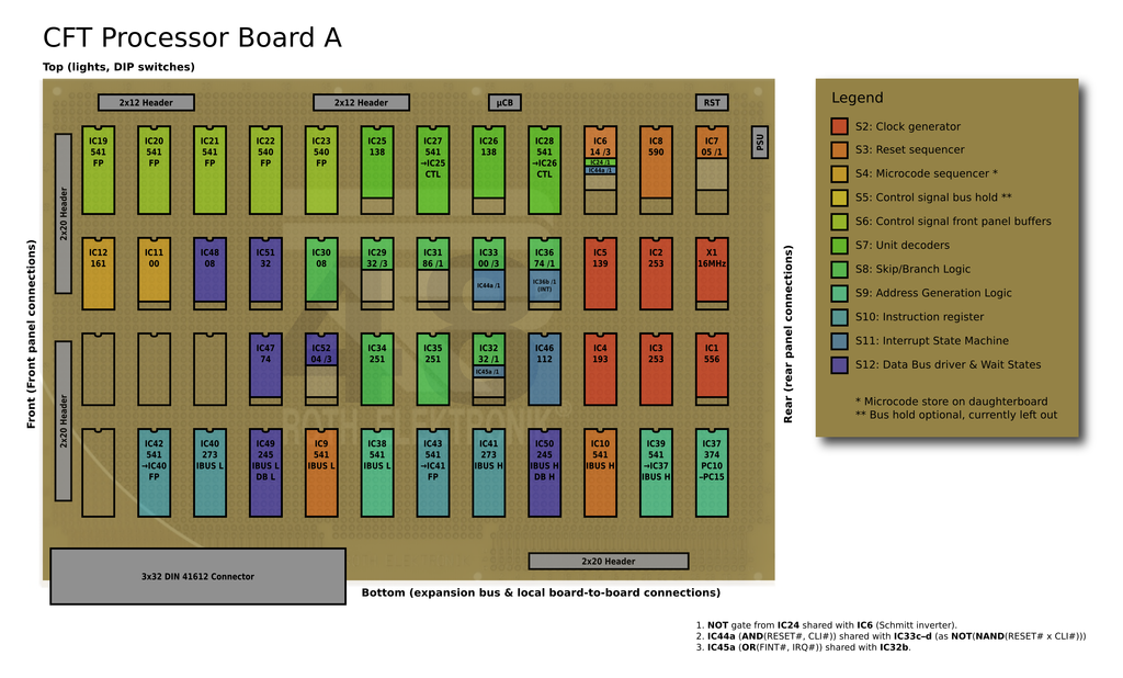
The original layout of the abandoned Processor Board A using point-to-point wired DIP packages on 6U Eurocard boards. This was abandoned in favour of a proper PCB and SMT components to save space and simplify my life.
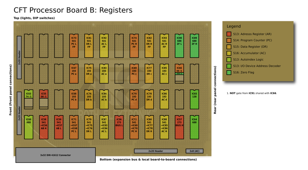
The original layout of the abandoned Processor Board B.
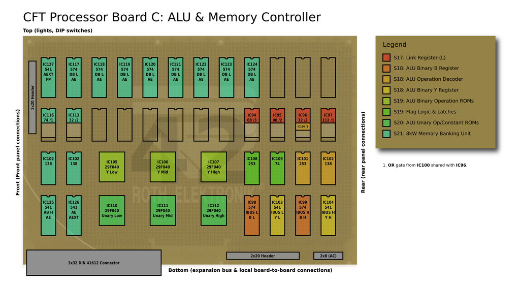
The original layout of the abandoned Processor Board C.
Several days into the 3U PCB design, it became obvious there wasn't enough space to route for DIP packages on two layers, and I had to switch to SMT components. They fit, but the only way was to promote the Microcode Store daughterboard to a full board.
The final (or nearly so) revisions of the Processor Boards ended up looking like this:
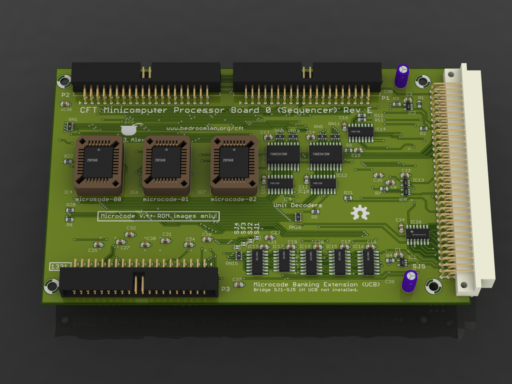
A render of the final layout of PB0, the microcode sequencer board.
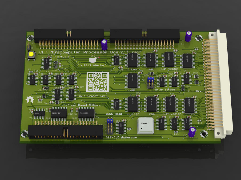
A render of the final layout of PB1, the control unit board.
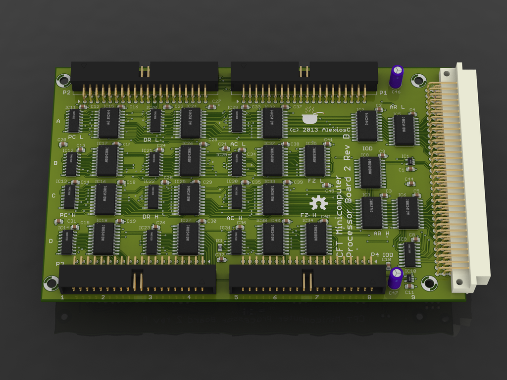
A render of the final layout of PB2, the register board.
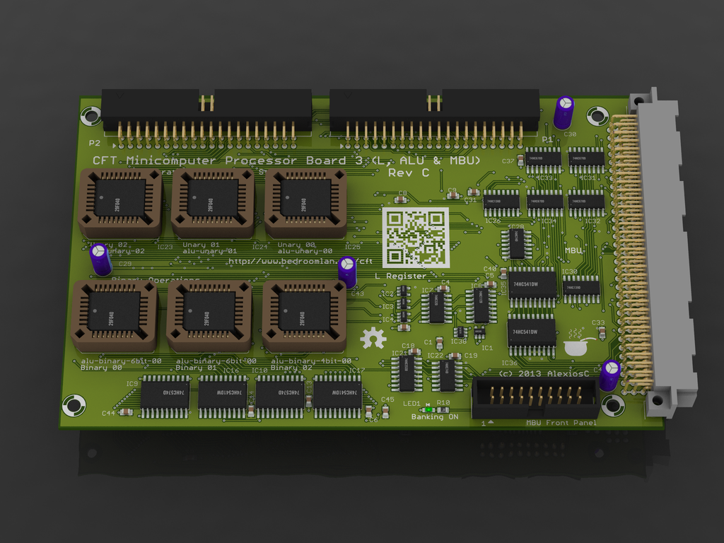
A render of the final layout of PB3, the ALU board.
On all boards, the left (white) DIN41612 connector is the CFT Expansion bus. The two 40-pin connectors along the top edge are the local processor control bus. Connectors along the bottom edge carry buffered signals to drive the LEDs on the front panel.
The hardest thing to do while designing the surface-mount versions of the boards was allow components in ‘unusual’ orientations. Most of the boards have all ICs in the same orientation (pin 1 to the upper left), but smaller packages, and routing necessitated some to be rotated by 90 degrees. The tiny, five or six-pin SOT32 gates were placed every which way was more convenient without bothering much.
Out of date renders!
lease note that the renders are out of date. I initially did them for fun, to get re-accustomed with PovRay, learn radiosity, and because I wanted to check the feasibility of the design and get some confidence in its looks. Once the first boards started arriving, I stopped rendering boards. It took a long time, too!B4.3. Actual Construction of the Boards
For all boards, construction was laborious but relatively simple: I would pick out the best looking PCB of the batch by (cursory) visual inspection. I applied solder paste manually using a dispenser. I'd then place all the surface mount components one by one with a pair of tweezers. Once that was done, I used a cheap hot air rework station to heat up the board, paste (and components) until the magic happened. Here's a video of the magic (this is neither me nor the CFT, but you can get the idea):
On more complex boards like the PB2, the paste would warm up and get loose during placing, so I had to pate, place and heat the board one section at a time, while ensuring the components I'd previously soldered don't come loose because of the copper getting hot. Despite thermal relief pads, the power and ground planes still stored plenty of heat!
To make things even more interesting, most boards have components on both sides. Early on I learned it was A Good Idea to start on the rear side, since it's always less populated. Cringe if you must: I'd complete one side, then move on to the other one. When I applied heat to the working side, the smaller components on the upside down side would fall clean off. I learned to listen for the gentle tapping of 0805 resistors falling on the anti-static mat.
Eventually, I solved some of these problems by sticking the more restless components onto the board with Kapton tape, sandwiching them between the working board and a sacrificial PCB and clamping them together, et cetera. Afterwards, I carefully inspected the backside with a loupe to make sure nothing had moved.
For multiple-pinned packages like resistor networks (those were tiny!) and ICs, I applied flux and reheated the solder pads with a soldering iron to collect excess solder and break any bridges between pins. That solved quite a few problems as I often managed to get minuscule, unmelted solder balls trapped in the tiny spaces between SOIC package legs.
Finally, I'd install through hole components in traditional lowest-height-first order. For most of the PBs, those were the ‘large’ filter capacitors near the card power inputs and the plugs.
When it was all done, I cleaned the boards with an isopropyl alcohol spray, and got a free high as a side-effect. Yes, I'm an idiot, I did it indoors without proper ventilation, even though it was a big open plan space. Don't do this in an unventilated space, kids!
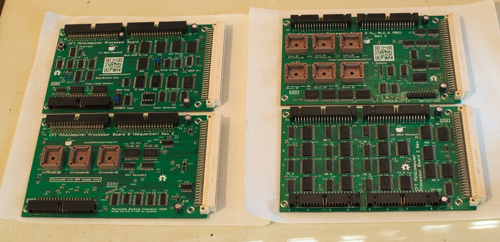
All four Processor Boards drying after construction and cleaning. Lower left: PB0, the microcode sequencer. Upper left: PB1, the Control Unit. Upper right: PB2, the Arithmetic and Logic Unit. Lower right: PB1, the register board. The ROMs ICs and clock oscillator haven't yet been installed in their sockets, but PB1 is sporting its jumpers (and some fine Kynar wire implementing last-minute bug fixes—it's near the Open Hardware logo)
Here are some colourised renders of the Gerber plot files for the processor boards, made to look like actual boards, but closely resembling the boards anyway!
B4.3.1. Processor Board 0 (PB0)
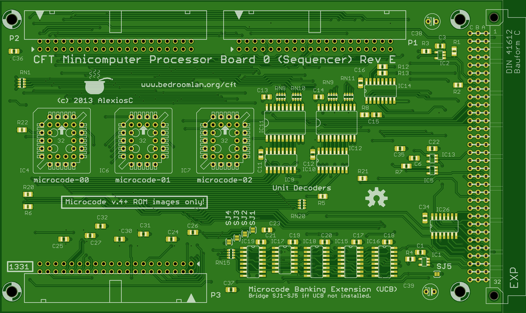
Processor Board 0. Top view.
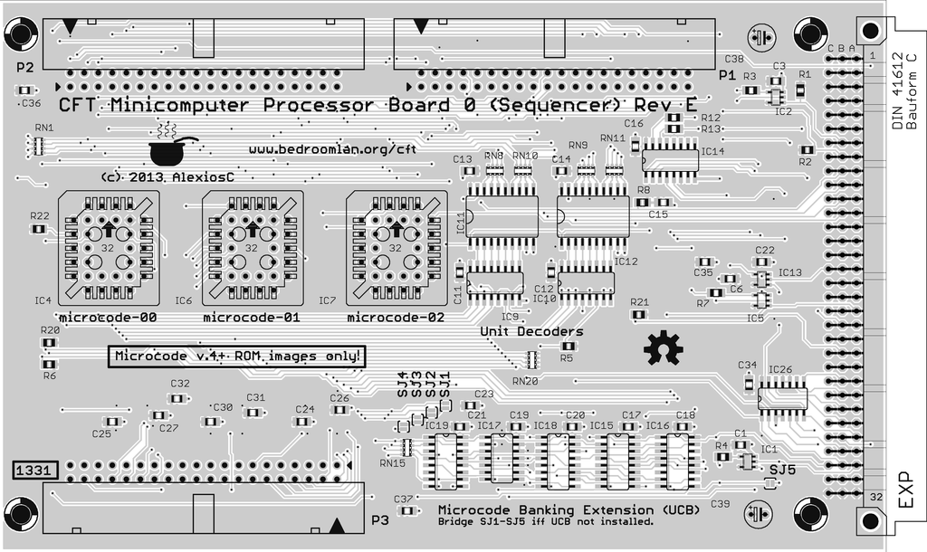
Processor Board 0. Top view, silkscreen.
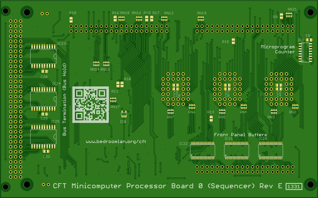
Processor Board 0. Bottom view.
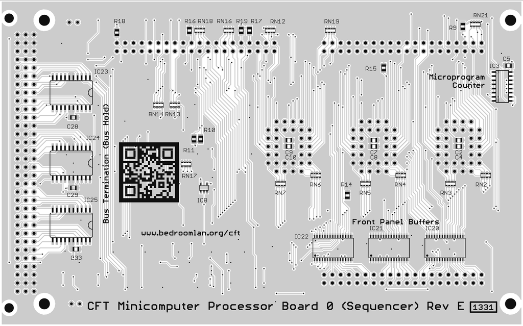
Processor Board 0. Bottom view, silkscreen.
B4.3.2. Processor Board 1 (PB1)
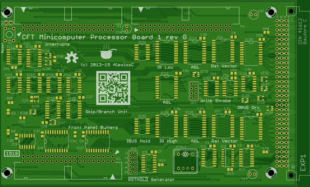
Processor Board 0. Top view.
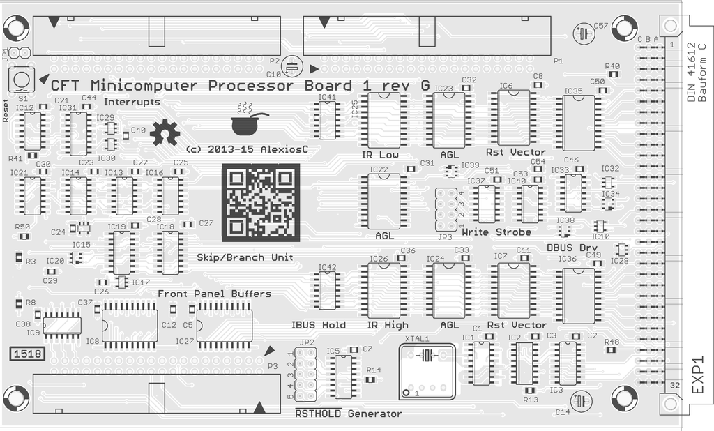
Processor Board 0. Top view, silkscreen.
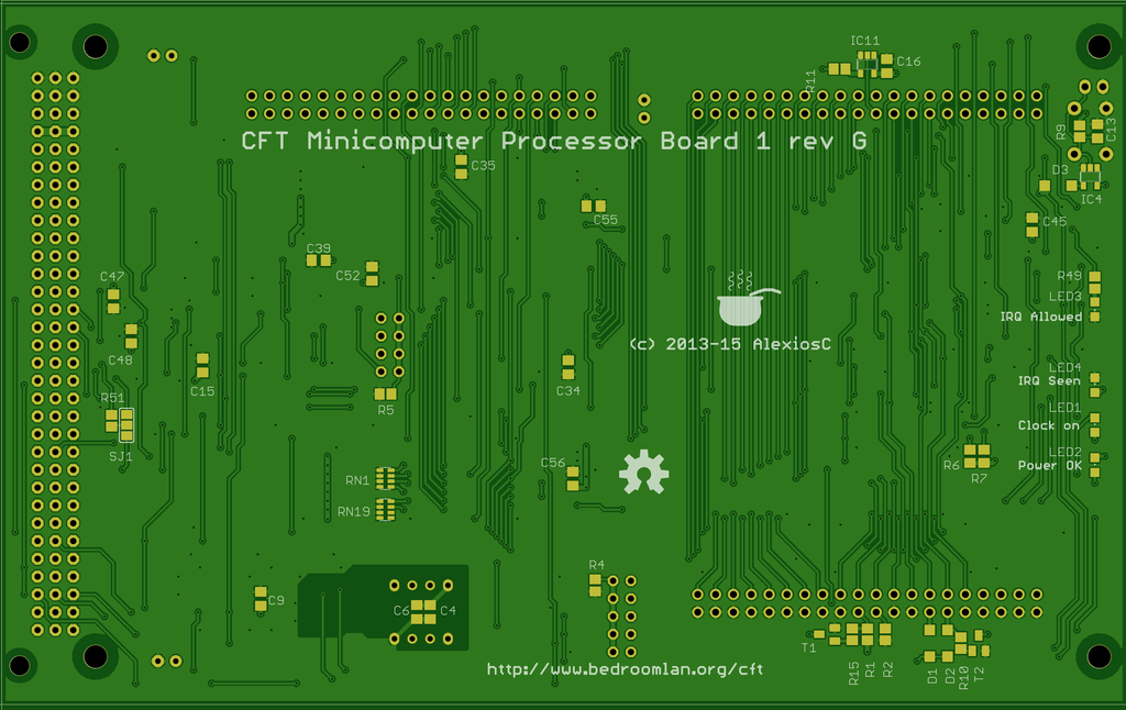
Processor Board 0. Bottom view.
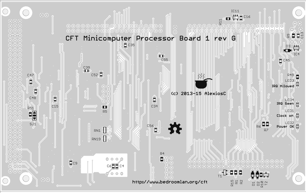
Processor Board 0. Bottom view, silkscreen.
B4.3.3. Processor Board 2 (PB2)
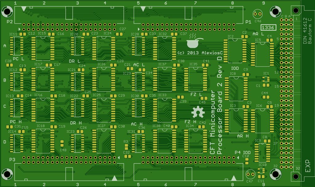
Processor Board 0. Top view.
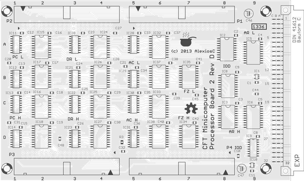
Processor Board 0. Top view, silkscreen.
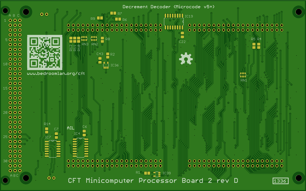
Processor Board 0. Bottom view.
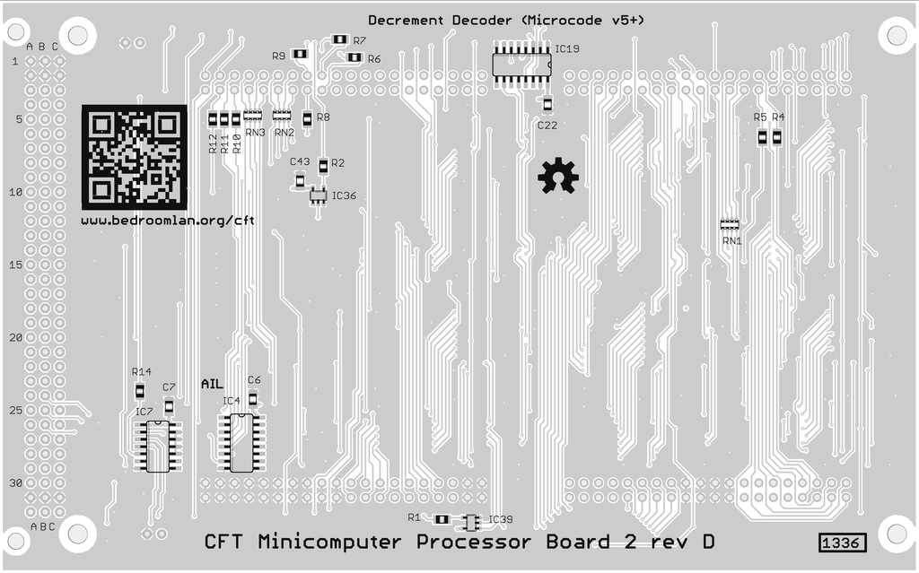
Processor Board 0. Bottom view, silkscreen.
B4.3.4. Processor Board 3 (PB3)

Processor Board 0. Top view.
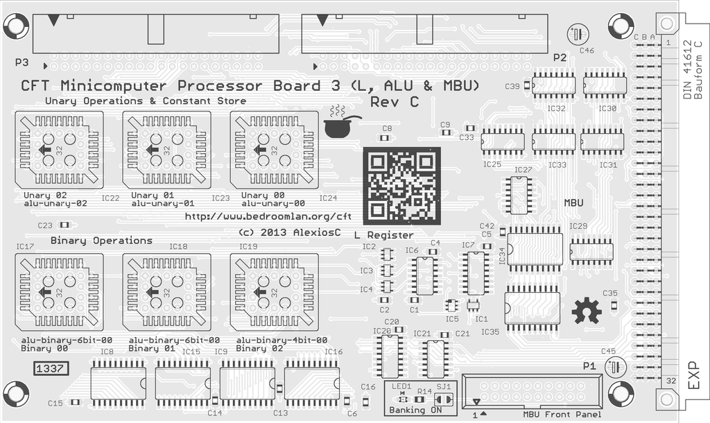
Processor Board 0. Top view, silkscreen.
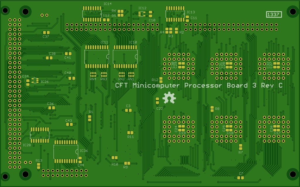
Processor Board 0. Bottom view.
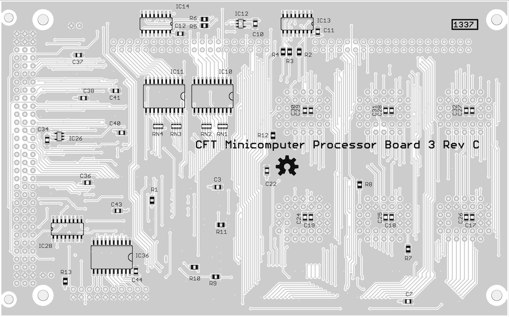
Processor Board 0. Bottom view, silkscreen.
